Electronic voltage switches. Simple electronic switch. Scheme, description. Electronic relay - schematic diagram
Almost every radio amateur has at least once used P2K switches, which can be single (with or without latching) or assembled in groups (without latching, independent latching, dependent latching). In some cases, it is more expedient to replace such switches with electronic ones assembled on TTL microcircuits. It is these switches that we will talk about.
Latching switch. The equivalent in digital circuitry of such a switch is a flip-flop with a counting input. When you press the button for the first time, the trigger goes into one stable state, and when you press it again, it goes into the opposite state. But it is impossible to directly control the counting input of the trigger with a button due to the bounce of its contacts at the moment of closing and opening. One of the most common methods of combating bounce is to use a switch button in conjunction with a static trigger. Let's take a look at Fig. 1.
Fig.1
In the initial state, the outputs of elements DD1.1 and DD1.2 are “1” and “0”, respectively. When you press the SB1 button, the very first closure of its normally open contacts switches the trigger assembled on DD1.1 and DD1.2, and contact bounce does not affect its further fate - in order for the trigger to return to its original state, it is necessary to apply a logical zero to its lower element . This can only happen when the button is released and again the chatter will not affect the reliability of the switching. Next, our static trigger controls a regular counter, which is switched by input C with the edge of the signal from output DD1.2.
The following circuit (Fig. 2) works similarly, but allows you to save one case, since the second half of the DD1 chip is used as a static trigger.

Fig.2
If the use of buttons with switching contacts is inconvenient, then you can use the diagram shown in Fig. 3.

Fig.3
It uses the chain R1, C1, R2 as a bounce suppressor. In the initial state, the capacitor is connected to the +5 V circuit and is discharged. When you press the SB1 button, the capacitor starts charging. As soon as it charges, a negative pulse will be generated at the input of the counting trigger, which will switch it. Since the charging time of the capacitor is much longer than the time of transient processes in the button and is about 300 ns, the bouncing of the button contacts does not affect the state of the trigger
Latching and Master Reset Switches. The circuit shown in Fig. 4 represents an arbitrary number of buttons with independent fixation and one general reset button.

Fig.4
Each switch is a static trigger, activated by a separate button. Since when even a short low level appears, the trigger unambiguously switches and is held in this position until the “reset” signal at the other input, a debouncing circuit for the button contacts is not needed. The reset inputs of all flip-flops are connected and connected to the SBL button, which is a common reset button. Thus, you can turn on each trigger with a separate button, but you can only turn it off all at once with the “Reset” button.
Latent Switches. In this scheme, each button turns on its static trigger and simultaneously resets all others. Thus, we get an analogue of the line of P2K buttons with dependent fixation (Fig. 5).

Fig.5
As in the previous circuit, each button turns on its own trigger, but at the same time it starts a reset circuit assembled on transistor VT2 and elements DK.3, DK.4. Let's consider the operation of this node. Suppose we need to enable the first trigger (elements D1.1, D1.2). When you press the SB1 button, a low level (since capacitor C1 is discharged) will switch the trigger (input of element D1.1). The capacitor will immediately begin to charge through the circuit SB1, R8. As soon as the voltage on it increases to approximately 0.7V, transistor VT1 opens, but for element D1.1 this voltage is still logical “0”.
The transistor will immediately switch the Schmidt trigger on elements DK.3, DK.4, which will generate a short pulse at the reset inputs of all triggers. All triggers will be reset (if they were turned on before), except for the first one, since logical “0” (voltage below 1 V) is still supplied to its upper input in the circuit through the SB1 button. Thus, the delay in the passage of the reset signal is sufficient to stop the contact bounce, but the reset will occur faster than we release the button that prohibits switching the corresponding trigger
An interesting and simple switch circuit with dependent latching can be built on the K155TM8 microcircuit (Fig. 6).

Fig.6
When power is applied, the R6, C1 chain resets all flip-flops and their direct outputs are set to a low logic level. At inputs D the level is also low, since they are all connected through their own button to the common wire. Let's assume the SB1 button is pressed. The input of the first trigger is set to “1” (thanks to R1), and the general clock input is set to “0” (via the switching contact of the button). So far, theoretically, nothing happens, since the microcircuit gates the data on a positive edge. But when the button is released, the data from the inputs will be copied into flip-flops - into 2, 3, 4 - “0”, into 1 - “1”, since the positive edge at input C appears before the upper contacts SB1 in the circuit are closed. When any other button is pressed, the cycle will repeat, but “1” will be written to the trigger whose button is pressed. This is in theory. In practice, due to contact bounce, the data from the input will be overwritten immediately after pressing the button and will not change when it is released.
All of the above schemes with dependent latching have one significant drawback, which is also characteristic of P2K switches - the ability to “snap” several buttons when they are pressed simultaneously. A circuit assembled on a priority encoder will allow you to avoid this (Fig. 7).

Fig.7
The circuit, of course, looks quite cumbersome, but in fact it consists of only three buildings without additional attachments and, importantly, does not require switching buttons. When you press the button, the priority encoder DD1 sets the binary code (inverse) of this button at its output and confirms it with the G “strobe” signal, which immediately writes data to the DD2 chip, operating in the mode of a four-bit parallel latch register. Here the code is inverted again (the outputs of the register are inverted) and goes to the usual binary decimal decoder DD3. Thus, the corresponding output of the decoder is set to a low level, which will remain unchanged until any other button is pressed. The impossibility of latching two buttons simultaneously is ensured by the priority circuit (I wrote more about the operation of the priority encoder). Since the K155IV1 microcircuit was designed to increase the bit capacity, it would be stupid not to take advantage of this and assemble a block of radio-latching switches for 16 buttons (Fig. 8).

Fig.8
I will not dwell on the operation of the circuit, since I have described in detail the principle of increasing the capacity of IV1. The pinout of the TTL power pins of the K155 series microcircuits (1533, 555, 133) can be seen.
Schemes of electronic power switches. Switch electronic circuit
ELECTRONIC SWITCH
The electronic switch circuit is based on the CD4013 chip, and has two stable states, ON and OFF. Once it's on, it stays on until you press the switch again. A short press of the SW1 button switches it to another state. The device will be useful for eliminating bulky and unreliable key switches or for remote control various electrical appliances.
Electronic relay - schematic diagram
The relay contacts can withstand high AC mains voltage as well as sufficient DC current, making the design suitable for appliances such as fan, light, TV, pump, electric motor direct current, and indeed any electronic project requires something like this electronic switch. The device operates from an AC mains voltage up to 250 V and switches loads up to 5 A.

Schema parameters and elements
- Power: 12 volts
- D1: power indicator
- D3: relay ON indicator
- CN1: power input
- SW1: switch

Transistor Q1 can be replaced with any similar structure with a current limit of at least 100 mA, for example KT815. You can take a car relay, or any other 12 V. If an electronic switch needs to be assembled in the form of a separate small-sized box, it makes sense to power the circuit from a small switching power supply, such as charging a mobile phone. You can increase the voltage from 5 to 12 V by replacing the zener diode on the board. If necessary, instead of a relay we install a powerful field-effect transistor, as is implemented in such a switch.
el-shema.ru
Electronic switch | all-he
The electronic switch circuit was designed to control loads remotely from a distance. We'll look at the complete structure of the device another time, but in this article we'll discuss a simple electronic switch circuit based on everyone's favorite 555 timer.

The circuit consists of the timer itself, a button without fixing a transistor as an amplifier and an electromagnetic relay. In my case, a 220 Volt relay with a current of 10 Amperes was used, these can be found in uninterruptible power supplies.

As power transistor You can use literally any medium and high power transistors. The circuit uses a reverse bipolar transistor (NPN), but I used a direct transistor (PNP), so you will need to change the polarity of the transistor connection, that is, if you are going to use a forward transistor, then the plus power is supplied to the emitter of the transistor, when using reverse transistors conductivity, minus power is supplied to the emitter.

For direct transistors, you can use transistors of the KT818, KT837, KT816, KT814 or similar series, for reverse transistors - KT819, KT805, KT817, KT815 and so on.
The electronic switch operates in a wide range of supply voltages, personally it supplied from 6 to 16 Volts, everything works clearly.

The circuit is activated when the button is briefly pressed, at this moment the transistor instantly opens, turning on the relay, and the latter, when closed, connects the load. The load is turned off only when pressed again. Thus, the circuit plays the role of a latching switch, but unlike the latter, it works exclusively on an electronic basis.

In my case, an optocoupler is used instead of a button, and the circuit closes when commanded from the control panel. The fact is that the signal to the optocoupler comes from a radio module, which was taken from a Chinese radio-controlled car. This system allows you to control multiple loads from a distance without much difficulty.
This scheme electronic switch always shows good operating parameters and works flawlessly - try it and see for yourself.

all-he.ru
Transistor switches - Meander - entertaining electronics
The main purpose of transistor switches, the circuits of which are presented to the attention of readers, is to turn on and off a DC load. In addition, it can also perform additional functions, for example, indicate its status, automatically turn off the load when the battery is discharged to the maximum permissible value or based on a signal from temperature, light sensors, etc. A switch can be made based on several switches. Current switching is carried out by a transistor, and control is carried out by one simple button with a short-circuit contact. Each press of the button changes the switch state to the opposite.
A description of a similar switch was given in, but two buttons are used for control. The advantages of the proposed switches include contactless load connection, virtually no current consumption when turned off, accessible elements and the possibility of using a small-sized button that takes up little space on the device panel. Disadvantages - own current consumption (several milliamps) in the on state, voltage drop across the transistor (fractions of a volt), the need to take measures to protect reliable contact in the input circuit from impulse noise (it can turn off spontaneously if the contact is briefly broken).
The circuit diagram of the switch is shown in Fig. 1. The principle of its operation is based on the fact that an open silicon transistor has a voltage at the transistor base-emitter junction of 0.5...0.7 V, and the collector-emitter saturation voltage can be 0.2...0.3 V. Essentially, this device is a trigger on transistors with different structure, controlled by one button. After supplying the supply voltage, both transistors are closed and capacitor C1 is discharged. When you press the SB1 button, the charging current of the capacitor C1 opens the transistor VT1, and after it the transistor VT2 opens. When the button is released, the transistors remain on, the supply voltage (minus the voltage drop across the transistor VT1) is supplied to the load and capacitor C1 continues to charge. It will charge to a voltage slightly greater than the base voltage of that transistor, since the collector-emitter saturation voltage is less than the base-emitter voltage.

Therefore, the next time you press the button, the base-emitter voltage on transistor VT1 will be insufficient to maintain it in the open state and it will close. Next, transistor VT2 will close, and the load will be de-energized. Capacitor C1 will discharge through the load and resistors R3-R5, and the switch will return to its original state. The maximum collector current of the transistor VT1 Ik depends on the current transfer coefficient h31e and the base current Ib: Ik = lb h3le. For the ratings and types of elements indicated on the diagram, this current is 100...150 mA. For the switch to work properly, the current consumed by the load must be less than this value.
This switch has two features. If there is a short circuit at the output of the switch, after briefly pressing the SB1 button, the transistors will open for a short time and then, after charging the capacitor C1, they will close. When the output voltage decreases to approximately 1 V (depending on the resistances of resistors R3 and R4), the transistors will also close, i.e. the load will be de-energized.
The second property of the switch can be used to build a discharge device for individual Ni-Cd or Ni-Mh batteries up to 1 V before combining them into a battery and further general charging. The device diagram is shown in Fig. 2. A switch on transistors VT1, VT2 connects a discharge resistor R6 to the battery, in parallel with which a voltage converter assembled on transistors VT3, VT4 is connected, powering the LED HL1. The LED indicates the status of the discharge process and is an additional load on the battery. Resistor R8 can change the brightness of the LED, as a result of which the current consumed by it changes. This way you can adjust the discharge current. As the battery discharges, the voltage at the input of the switch decreases, as well as at the base of the transistor VT2. The divider resistors in the base circuit of this transistor are selected in such a way that at an input voltage of 1 V, the voltage at the base will decrease so much that the transistor VT2 will close, and after it the transistor VT1 - the discharge will stop. With the element ratings indicated in the diagram, the discharge current adjustment interval is 40...90 mA. If resistor R6 is excluded, the discharge current can be changed in the range from 10 to 50 mA. When using a super-bright LED, this device can be used to build a flashlight with battery protection from deep discharge.

In Fig. Figure 3 shows another application of the switch - a timer. I used it in a portable device - a tester of oxide capacitors. An HL1 LED is additionally introduced into the circuit, which indicates the status of the device. After switching on, the LED lights up and capacitor C2 begins to charge with the reverse current of diode VD1. At a certain voltage, transistor VT3 will open on it, which will short-circuit the emitter junction of transistor VT2, which will lead to the device turning off (the LED will go out). Capacitor C2 will quickly discharge through diode VD1, resistors R3, R4 and the switch will return to its original state. The holding time depends on the capacitance of capacitor C2 and the reverse current of the diode. With the elements indicated in the diagram, it is about 2 minutes. If instead of capacitor C2 we install a photoresistor, thermistor (or other sensors), and instead of a diode - a resistor, we get a device that will turn off when the light, temperature, etc. changes.

If the load contains large capacitors, the switch may not turn on (this depends on their capacitance). The diagram of a device that does not have this drawback is shown in Fig. 4. Another transistor VT1 has been added, which performs the function of a key, and two other transistors control this key, which eliminates the influence of the load on the operation of the switch. But in this case, the property of not turning on if there is a short circuit in the load circuit will be lost. The LED performs a similar function. With the component ratings indicated in the diagram, the base current of transistor VT1 is about 3 mA. Several transistors KT209K and KT209V were tested as a key. They had base current transfer coefficients from 140 to 170. At a load current of 120 mA, the voltage drop across the transistors was 120...200 mV. At a current of 160 mA - 0.5...2.2 V. The use of a composite transistor KT973B as a switch made it possible to significantly increase the permissible load current, but the voltage drop across it was 750...850 mV, and at a current of 300 mA the transistor was slightly heated. When turned off, the current consumption is so small that it could not be measured using the DT830B multimeter. In this case, the transistors were not pre-selected for any parameters.

In Fig. Figure 5 shows a diagram of a three-channel dependent switch. It combines three switches, but if necessary their number can be increased. A short press on any of the buttons will turn on the corresponding switch and connect the corresponding load to the power source. If you press any other button, the corresponding switch will turn on and the previous one will turn off. Pressing the next button will turn on the next switch, and the previous one will turn off again. When you press the same button again, the last working switch will turn off and the device will return to its original state - all loads will be de-energized. The switching mode is provided by resistor R5. When a switch is turned on, the voltage across this resistor increases, which leads to the closing of the previously turned on switch. The resistance of this resistor depends on the current consumed by the switches themselves, in this case its value is about 3 mA. Elements VD1, R3 and C2 ensure the passage of the discharge current of capacitors SZ, C5 and C7. Through resistor R3, capacitor C2 discharges in pauses between button presses. If this circuit is eliminated, only the on and switch modes remain. By replacing resistor R5 with a wire jumper, we get three independently operating devices.

The switch was supposed to be used in a switch television antennas with amplifiers, but with the advent cable television the need for it disappeared, and the project was not implemented in practice.
The switches can use transistors of the most different types, but they must meet certain requirements. First, they all must be silicon. Secondly, transistors that switch the load current must have a saturation voltage Uk-e us no more than 0.2...0.3 V, the maximum permissible collector current Ikmax must be several times greater than the switched current, and the current transfer coefficient h31e sufficient so that at a given base current the transistor is in saturation mode. Of the transistors I have, the transistors of the KT209 and KT502 series have proven themselves well, and somewhat worse - the KT3107 and KT361 series.
The resistor resistances can be varied within significant limits. If greater efficiency is required and there is no need to indicate the state of the switch, an LED is not installed, and the resistor in the collector circuit VTZ (see Fig. 4) can be increased to 100 kOhm or more, but it must be taken into account that this will reduce the base current of the transistor VT2 and the maximum load current. Transistor VTZ (see Fig. 3) must have a current transfer coefficient h31e of more than 100. The resistance of resistor R5 in the charging circuit of capacitor C1 (see Fig. 1) and similar ones in other circuits can be in the range of 100.. 470 kOhm. Capacitor C1 (see Fig. 1) and similar ones in other circuits should have a low leakage current; it is advisable to use oxide semiconductor series K53, but oxide ones can also be used, and the resistance of resistor R5 should be no more than 100 kOhm. If the capacitance of this capacitor increases, the performance will decrease (the time after which the device can be turned off after being turned on), and if it is decreased, the clarity of operation will decrease. Capacitor C2 (see Fig. 3) is only an oxide semiconductor. Buttons - any small ones with self-return. The L1 coil of the converter (see Fig. 2) is used from the line linearity regulator of a black-and-white TV; the converter also works well with a choke on the W-shaped magnetic circuit from a CFL. You can also use the recommendations given in. Diode VD1 (see Fig. 5) can be any low-power diode, either silicon or germanium. Diode VD1 (see Fig. 3) must be germanium.
Installation requires devices, the diagrams of which are shown in Fig. 2 and fig. 5, the rest do not need adjustment if there are no special requirements and all parts are in working order. To set up a discharge device (see Fig. 2), you will need a power source with an adjustable output voltage. First of all, instead of resistor R4, a variable resistor with a resistance of 4.7 kOhm (at maximum resistance) is temporarily installed. Connect the power source, having previously set the voltage at its output to 1.25 V. Turn on the discharge device by pressing the button and set the required discharge current using resistor R8. After this, a voltage of 1 V is set at the output of the power source, and using an additional variable resistor, the device is turned off. After this, you need to check the shutdown voltage several times. To do this, you need to increase the voltage at the output of the power source to 1.25 V, turn on the device, then you need to smoothly reduce the voltage to 1 V, observing the moment it turns off. Then measure the introduced part of the additional variable resistor and replace it with a constant one with the same resistance.
All other devices can also implement a similar shutdown function when the input voltage drops. The setup is done in the same way. In this case, one must keep in mind the fact that near the turn-off point, the transistors begin to close smoothly and the current in the load will also gradually decrease. If there is a radio receiver as a load, this will manifest itself as a decrease in volume. Perhaps the recommendations described in will help solve this problem.
Setting up the switch (see Fig. 5) comes down to temporary replacement fixed resistors R3 and R5 for variables with a resistance 2...3 times greater. By successively pressing the buttons, using resistor R5, reliable operation is achieved. After this, by repeatedly pressing the same button using resistor R3, a reliable shutdown is achieved. Then the variable resistors are replaced with constant ones, as mentioned above. To increase noise immunity, ceramic capacitors with a capacity of several nanofarads must be installed in parallel with resistors R7, R13 and R19.
LITERATURE
- Polyakov V. Electronic switch protects battery. - Radio, 2002, No. 8, p. 60.
- Nechaev I. Electronic match. - Radio, 1992, N° 1, p. 19-21.
You might be interested in this:
meandr.org
Electronic switch circuit on CD4027B chip
Electronic switch circuit - replaces a mechanical switch

Electronic switch circuit is simple and inexpensive electronic circuit with a cheap tact button can control the load's power on and off. The circuit replaces a more expensive and larger mechanical latching switch. The button starts the standby multivibrator. The output of the multivibrator switches a counting trigger, the logical output level of which, changing after each button press, switches the power supply to the load.
There are several different options for implementing this scheme. An option that uses two J-K flip-flops IC1 and IC2 of one CD4027B chip is shown in Figure 1. Feedback coming from an RC circuit connected to the IC1 output to the reset input turns this flip-flop into a standby multivibrator. The J input of the IC1 microcircuit is connected to the power bus, and the K input is connected to ground, therefore, at the leading edge of the clock pulse, “log” is set at its output. 1". Tact button is connected between the clock input of the IC1 chip and ground. In the same way, the button can be connected between the clock input and the positive VDD power bus. Connecting the J and K pins high turns IC2 into a counting flip-flop. IC2 is switched by the rising edge of the output signal IC1.


You can understand the operation of the circuit by looking at the timing diagrams at its different points, shown in Figure 2. When you press the button on the clock input IC1, bounce pulses begin to arrive, the leading edge of the first of which sets the output to a high level. Capacitor C1 begins to charge through resistor R1 to the “log” level. 1". At the same moment, the rising edge of the pulse arriving at the clock input of the counting trigger IC2 switches the state of its output. When the voltage across capacitor C1 reaches the RESET input threshold of IC1, the trigger is reset and the output level goes low.
After this, C1 is discharged through R1 to the “log” level. ABOUT". The charge and discharge rates of C1 are the same. The duration of the multivibrator output pulse must exceed the time the button is pressed and the duration of the bounce. By adjusting the tuning resistor R1, this duration can be changed in accordance with the type of button used. The complementary outputs of IC2 can be used to control transistor power switches, relays, or switching regulator switching pins. The circuit operates from 3V to 15V and can control power to analog and digital devices.
Do it yourself
usilitelstabo.ru
Circuits of electronic power switches | Techniques and Programs
It would seem that it couldn’t be easier, I turned on the power and the device containing the MK started working. However, in practice there are cases when a conventional mechanical toggle switch is not suitable for these purposes. Illustrative examples:
The microswitch fits well into the design, but it is designed for low switching current, and the device consumes an order of magnitude more;
It is necessary to perform remote power on/off using a logic level signal;
The power switch is made in the form of a touch (quasi-touch) button;
It is required to perform a “trigger” power on/off by repeatedly pressing the same button.
For such purposes, special circuit solutions are needed, based on the use of electronic transistor switches (Fig. 6.23, a...m).

Rice. 6.23. Scheme electronic inclusion nutrition (start):
a) SI is a “secret” switch used to limit unauthorized access to a computer. A low-power toggle switch opens/closes field-effect transistor VT1, which supplies power to the device containing the MK. When the input voltage is higher than +5.25 V, it is necessary to install an additional stabilizer in front of the MK;
b) turning on/off the +4.9 V power supply with a digital ON-OFF signal through the DDI logic element and switching transistor VT1
c) low-power “quasi-touch” button SB1 triggers on/off the +3 V power supply through the DDL chip. Capacitor C1 reduces contact “bounce.” The HL1 LED indicates the flow of current through the VTL key transistor. Advantage of the circuit very low self-current consumption in the off state;

Rice. 6.23. Electronic power supply circuits (continued):
d) supply voltage +4.8 V with a low-power SBI button (without self-reset). The +5 V input power supply must have current protection so that the VTI transistor does not fail when short circuit under load;
e) switching on voltage +4.6 V external signal£/in. Galvanic isolation is provided on the optocoupler VU1. The resistance of the resistor RI depends on the amplitude £/in;
e) buttons SBI, SB2 must be self-returning, they are pressed in turn. The initial current passing through the contacts of the SB2 button is equal to the total load current in the +5 V circuit;
g) L. Coyle’s diagram. The VTI transistor automatically opens when the XP1 plug is connected to the XS1 socket (due to resistors R1, R3 connected in series). At the same time, the main device is supplied sound signal from the audio amplifier through elements C2, R4. The RI resistor may not be installed if the active resistance of the “Audio” channel is low;
h) similar to Fig. 6.23, in, but with the key on field effect transistor VT1. This allows you to reduce your own current consumption both in the off and on states;

Rice. 6.23. Electronic power supply circuits (end):
i) scheme for activating MK for a strictly fixed period of time. When the contacts of switch S1 are closed, capacitor C5 begins to charge through resistor R2, transistor VTI opens, and the MK turns on. As soon as the voltage at the gate of transistor VT1 decreases to the cutoff threshold, the MK turns off. To turn it on again, you need to open contacts 57, wait a short pause (depending on R, C5) and then close them again;
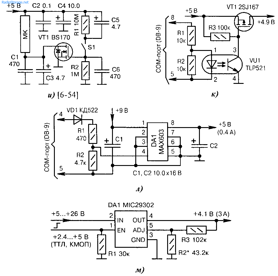
j) galvanically isolated switching on/off the +4.9 V power supply using signals from the COM port of the computer. Resistor R3 maintains the closed state of transistor VT1 when the optocoupler VUI is “off”;
k) remote on/off of the integrated voltage stabilizer DA 1 (Maxim Integrated Products) via the computer's COM port. The +9 V supply can be reduced down to +5.5 V, but in this case it is necessary to increase the resistance of resistor R2 so that the voltage at pin 1 of the DA I chip becomes greater than at pin 4;
l) voltage stabilizer DA1 (Micrel) has a power-on input EN, which is controlled by a HIGH logic level. The RI resistor is needed so that pin 1 of the DAI chip does not “hang in the air,” for example, in the Z-state of the CMOS chip or when the connector is unplugged.
It would seem that it couldn’t be easier, I turned on the power and the device containing the MK started working. However, in practice there are cases when a conventional mechanical toggle switch is not suitable for these purposes. Illustrative examples:
- the microswitch fits well into the design, but it is designed for low switching current, and the device consumes an order of magnitude more;
- it is necessary to remotely turn on/off the power using a logical level signal;
- The power switch is made in the form of a touch (quasi-touch) button;
- It is required to perform a “trigger” power on/off by repeatedly pressing the same button.
For such purposes, special circuit solutions are needed, based on the use of electronic transistor switches (Fig. 6.23, a...m).
Rice. 6.23. Electronic power supply circuits (beginning):
a) SI is a “secret” switch used to restrict unauthorized access to a computer. A low-power toggle switch opens/closes field-effect transistor VT1, which supplies power to the device containing the MK. When the input voltage is higher than +5.25 V, it is necessary to install an additional stabilizer in front of the MK;
b) turning on/off the +4.9 V power supply with a digital ON-OFF signal through the DDI logic element and switching transistor VT1
c) low-power “quasi-touch” button SB1 triggers on/off the +3 V power supply through the DDL chip. Capacitor C1 reduces contact “bounce.” The HL1 LED indicates the flow of current through the VTL key transistor. The advantage of the circuit is its very low self-current consumption in the off state;

Rice. 6.23. Electronic power supply circuits (continued):
d) supply voltage +4.8 V with a low-power SBI button (without self-reset). The +5 V input power supply must have current protection so that the VTI transistor does not fail if there is a short circuit in the load;
e) switching on the +4.6 V voltage using an external signal £/in. Galvanic isolation is provided on the optocoupler VU1. The resistance of the resistor RI depends on the amplitude £/in;
e) buttons SBI, SB2 must be self-returning, they are pressed in turn. The initial current passing through the contacts of the SB2 button is equal to the total load current in the +5 V circuit;
g) L. Coyle’s diagram. The VTI transistor automatically opens when the XP1 plug is connected to the XS1 socket (due to resistors R1, R3 connected in series). At the same time, a sound signal from the audio amplifier is supplied to the main device through elements C2, R4. The RI resistor may not be installed if the active resistance of the “Audio” channel is low;
h) similar to Fig. 6.23, v, but with a switch on the field-effect transistor VT1. This allows you to reduce your own current consumption both in the off and on states;
Rice. 6.23. Electronic power supply circuits (end):
i) scheme for activating MK for a strictly fixed period of time. When the contacts of switch S1 are closed, capacitor C5 begins to charge through resistor R2, transistor VTI opens, and the MK turns on. As soon as the voltage at the gate of transistor VT1 decreases to the cutoff threshold, the MK turns off. To turn it on again, you need to open contacts 57, wait a short pause (depending on R, C5) and then close them again;
j) galvanically isolated switching on/off the +4.9 V power supply using signals from the COM port of the computer. Resistor R3 maintains the closed state of transistor VT1 when the optocoupler VUI is “off”;
k) remote on/off of the integrated voltage stabilizer DA 1 (Maxim Integrated Products) via the computer's COM port. The +9 V supply can be reduced down to +5.5 V, but in this case it is necessary to increase the resistance of resistor R2 so that the voltage at pin 1 of the DA I chip becomes greater than at pin 4;
l) voltage stabilizer DA1 (Micrel) has a power-on input EN, which is controlled by a HIGH logic level. The RI resistor is needed so that pin 1 of the DAI chip does not “hang in the air,” for example, in the Z-state of the CMOS chip or when the connector is unplugged.
Now we will look at the TDA1029 chip produced by the small European company Philips. This small European company has a small division producing small semiconductor devices. I myself was very surprised - it turned out that Philips produces something else besides mobile phones and other household rubbish.
So, let's get to the point.
The above microcircuit is a signal selector for various amplifiers. The 16-leg case accommodates 4 stereo inputs and 1 stereo output.
Main settings the following:
In general, it’s very good, isn’t it? The following goodies are also built into the microcircuit: silent switching of inputs, protection of outputs from short circuits.
Let's look at the connection diagram:
In principle, there is nothing special to comment on. To our left are the entrances and to our right is the exit. Also on the right are the output switches. If none of the switches is closed, then the signal is taken from the first input - the topmost one in the circuit. If one of the switches closes, the selector switches to the corresponding state. Switches can be of any type - no sound signal passes through them, so you can put whatever comes to mind - that’s what’s good about an electronic switch - it doesn’t have contacts that oxidize or wear through over time. Very convenient in all respects. We solder and use it.
List of radioelements
| Designation | Type | Denomination | Quantity | Note | Shop | My notepad |
|---|---|---|---|---|---|---|
| Chip | TDA1029 | 1 | To notepad | |||
| C1-C8, C10 | Capacitor | 0.22 µF | 9 | To notepad | ||
| C9 | Electrolytic capacitor | 100 µF 20 V | 1 | To notepad | ||
| R1-R8 | Resistor | 470 kOhm | 8 | To notepad | ||
| S1-S3 | Switch | 3 |
Finally found time to write an article about switches. In the article
I have already mentioned how you can use a servo drive that is left without gears and an electric motor, but retains the functionality of the controller. Such a servo drive is not always cost-effective to repair, but it is quite suitable for “crafts”.
And if there are just one or two options for simple regulators from a servo drive, then more than one or two different switches (switches, switches, switches) can be created.
Looking ahead, I’ll make a reservation that currently you can buy remote-controlled switches, for example these:
These are ready-made products that allow you to install them on the model and use them “without racking your brains about what_and_how.”
And this is a huge plus! But there are also disadvantages:
- almost all of them switch at a fixed setting of %РРМ, usually -100%...+100% without the ability to set an arbitrary switching level;
- narrow functionality, and it is not always possible to adapt the finished product to your needs;
- long wait for delivery and additional payment for it;
- as a rule, there is practically no way to repair the device, and buying a new switch means waiting weeks again.
Now about “homemade products”.
First of all, I would like to point out a rather big drawback: assembly requires the ability to work with a soldering iron and at least basic knowledge of electronics. Also, “homemade” ones are clearly inferior in weight and size to the above switches. However, using the appropriate components and having skills in assembling radio-electronic devices, you can “fit” everything into the dimensions of a matchbox.
The advantages I see are that:
- a servo drive with “dead” mechanics will still serve, albeit in a different capacity;
- the ability to design a switch specifically for your goals and objectives;
- the ability to set an arbitrary on/off point, which makes it possible to make any switches during hardware mixing with any channel, for example, turn on the landing lights on the aircraft at a low throttle level;
- the ability to create control automation elements without the use of specialized controllers;
- no need to wait for weeks for the parcel and pay for delivery;
- the switches use widely available components that are available in radio parts stores in your city;
- maintainability of the device;
The devices discussed in the article are designed for the novice radio amateur... Hm…. electronic engineer...,
are not difficult to manufacture and do not require knowledge of programming microprocessor devices - it is enough to simply count the required legs of the microcircuit and solder everything in accordance with the pin designations. Assembled from widely available serviceable parts, the switches begin to work immediately, without requiring configuration of operating modes. The only thing is that you need to set the desired switching threshold.
The article provides a far from complete list of options for implementing switches with different functionality.
All switches made on the basis of a servo drive controller retain their state after the loss of the control signal (for example, turning off the remote control panel); to change the state of the switch in this case, it is recommended to use (if the remote control receiver does not have a built-in FS function) a device similar to these :
The switches described in this article use the SG90 servo controller. The cost of a new servo drive is from seventy rubles.
How to remove the controller from the servo housing, short description connections, installation procedure for the controller neutral, etc. can be viewed at the link indicated at the beginning of this article (article “Servo drive. Life after death”).
All switches based on a servo drive controller can be hardware-mixed (via a Y-cable, for example) with any RC channel.
The numbering of the outputs of the control signal source and the inputs of the servo drive controller in the diagrams is given arbitrarily, but corresponds to the order of location in the connecting cable.
The numbering of the controller outputs in the diagrams is given conditionally; the outputs are equivalent, but operate inversely with respect to each other. The choice of a specific output for use in the circuit is determined by the problems being solved. If necessary, you just need to swap the controller outputs or the polarity of connecting the extreme terminals of the position sensor on the controller board.
In the diagrams the markings “A1” and “A2” indicate
A1 is a RU receiver (or servotester), whose diagram shows the outputs of one arbitrary channel.
A2 is the servo drive controller from which one or another switch will be made.
The cost of these units is not given, since it is assumed that they are already available.
The ratings and types of components are indicated in the diagrams and descriptions.
The average cost of components in the above diagrams is approximately as follows:
Diode KD522 – 5 RUR/piece
Transistor optocoupler - 20rub/piece
Transistor KT315G – 17rub/piece
Mosfet transistor 55A/65V – 85rub/piece
Mosfet transistor 0.4A/400V – 40rub/piece
Constant resistor, 0.25W – 5rub/piece
Variable resistor – 38rub/piece
Relay – 63rub/piece
Cost in stores in our region.
1. Relay switch.
In Fig. Figure 1 shows a simple relay switch consisting of a servo drive controller, to the output of which an electromagnetic relay is connected instead of a microelectric motor. Relay K1 is connected via diode VD1.
The diode switching polarity determines the section of the %PPM regulation range to the left and right of the “neutral”, at which the relay will be switched on (see diagram 1). 
Principle of operation:
When changing the task from the control panel, the voltage increases (PWM regulation at the controller output) on the winding of relay K1. When the relay response voltage is reached, the latter turns on and with its contacts switches the electrical circuit of the actuator. The moment the relay is turned on is adjusted by the position sensor of the servo drive controller at a given level of %PPM. When the voltage on the relay coil decreases and the return voltage is reached, the relay turns off.
There is no neutral position.
The relay should be selected with an operating voltage (operating voltage) of 3.4-4.5V and an operating coil current of up to 50mA.
Such a switch can be used for remote on/off various devices(model lighting devices, engine ignition systems, etc.). Relay contacts can also be used in various automatic control schemes.
By connecting two relays in parallel to the output of the servo drive controller through back-to-back diodes (Fig. 2), you can obtain a relay switch with a neutral position electrical circuit.
Principle of operation:
When changing the task from the control panel to the right or left of the “neutral”, the voltage increases (PWM regulation at the controller output) on the winding of the corresponding relay, depending on the direction of current flow at the controller output. When the relay response voltage is reached (in accordance with the “direction” of the diode), the latter turns on and with its contacts switches the electrical circuit of the actuator.
When the voltage on the relay coil decreases to the return voltage, the relay turns off. In the “neutral” position of the control element on the control panel, both relays are switched off (see diagram 2). 
There is a neutral position.
Galvanic isolation from the switched electrical circuit is ensured by the use of a relay contact group that is not electrically connected to the control circuit.
Such a switch can be used, for example, to change the direction of rotation of low-power electric motors with the ability to stop them. To switch high power, you will have to install more powerful repeater relays.
DC Motor Control: 
AC Motor Control ( the circuit with ESC has not been tested, the behavior of the regulator during such switching is unknown!!!
However, for the three-phase motor itself, the circuit works): 
Considering that relays K1 and K2 in normal mode can never be turned on simultaneously, no additional interlocks are required.
The disadvantage of the circuit lies in the PWM regulation of the output voltage of the servo controller. Due to the pulsed nature of the output voltage, relay bounce may occur. The presence of bounce depends on the relay return time - whether it “has time” to return to its original state or not during the pause between PWM pulses. The situation can be somewhat improved by switching on electrolytic capacitors in parallel with the relay coils, but it should be remembered that increasing the capacitance of these capacitors increases the relay switch-off time after the switch-off command is given.
It is worth noting that switches with a relay connected directly to the outputs of the servo drive controller are, unfortunately, critical to the choice of relay based on electrical characteristics - the required relays may simply not be on sale.
The use of an external key to control the relay significantly expands the possibilities for choosing operating voltages and currents of relay windings. The external switch, as a rule, is made of a bipolar or field-effect transistor (for high values of the operating current of the relay winding, it is recommended to use so-called “mosfets”). The choice of a key element is made based on the parameters of its load, i.e. electrical characteristics relay.
There are practically no restrictions in the choice of relays compared to the switches shown in Fig. 1,2. In Fig. Figure 5 shows a diagram of such a switch.
Principle of operation:
When the control element of the RU channel (stick on the RU remote control, servo tester regulator) deviates from the “neutral”, suppose to the left, a positive voltage appears at pin 4 of module A2, which through resistor R1 is supplied to the base of transistor VT1, as a result of which the latter opens and supplies voltage to the winding of relay K1, which, with its contacts K1.1, switches the electrical circuits of the actuator. When the control element of the RU channel returns to the “neutral”, or in this case, to the right of it, transistor VT1 closes, de-energizing the relay winding (see diagram 3).

Resistor R2 serves to reliably close the transistor in the absence of control voltage.
Capacitor C1 (with a capacity of 10...50 μF) is used to smooth out voltage ripples at the switch input (and as we remember, there is PWM regulation). Diode VD1 serves to protect the transistor from breakdown by self-induction currents of the relay and is selected based on the electrical parameters of the relay: at least three times the voltage reserve and two times the current reserve.
The moment the relay is turned on is adjusted by the position sensor of the servo drive controller at a given level of %PPM.
When using pin 5 of the controller, the switch operation algorithm will change to the opposite.
A similar cascade (K2) can be connected to pin 5 of the controller. Both relays will work inversely with respect to each other.
There is no neutral position.
It is possible to set an arbitrary switching threshold throughout the entire %PPM regulation range.
Galvanic isolation from the switched electrical circuit is ensured by the use of a relay contact group that is not electrically connected to the control circuit.
When choosing a relay, you should choose operating voltage windings are 10-20% lower than the supply voltage, which is due to the voltage drop at the junction of the bipolar transistor. The relay operation current is no more than 70mA.
For more powerful relays, you can use a switch implemented on a field-effect transistor - mosfet (Fig. 6).
The diode should be selected according to the characteristics of the relay coil. 
The supply voltage may differ from that shown in the diagram depending on the electrical characteristics of the relay.
Unfortunately, there is nothing to shoot video with, I tried it with a camera - the quality is absolutely no good. Still, I decided to insert one video - the kit is not visible there, but you can understand how to set the switching threshold.
Another option for a relay switch is a relay switch with a neutral position (Fig. 7).
Transistor optocouplers are used to interface the servo drive controller with power switches (Fig. 7a).


Principle of operation:
When the task is changed from the control panel to the right or left of the “neutral”, the corresponding LED inside the optocoupler lights up, which affects the optotransistor in the same optocoupler in the executive part of the switch (Fig. 7b).
In this case, when the %PPM setting changes, say, to the left of the “neutral”, a negative voltage is established at pin 5 relative to pin 4 of the controller, which is supplied through diode VD2 to the LED of optocoupler DA2.1, causing it to glow. Similarly, when the %PPM setting changes in the opposite direction from the “neutral” (to the right), a positive voltage is established at pin 5 relative to pin 4 of the controller, which is supplied through the diode VD1 to the LED of the optocoupler DA1.1, causing it to glow.
In “neutral” there is no voltage at pin 5 relative to pin 4 of the controller and both LEDs are off.
Diodes VD1 and VD2 protect the optocoupler LEDs from reverse voltage. Resistor R1 limits the current through the LEDs. Its resistance is selected based on the permissible current through the LED of the optocoupler in accordance with the recommendations of its manufacturer.
When the transistor of the optocoupler DA1 is illuminated, the transistor DA1.2 opens and supplies the supply voltage to the input of the transistor switch VT1, opening it. The circuit and operation of the key is described above and I see no reason to duplicate the text.
Optocoupler DA2 works similarly. In the neutral position, when none of the optocoupler LEDs are lit, transistors DA1.2 and DA2.2 are closed, transistors VT1 and VT2 are also closed, and both relays are turned off.
The relay switching moment is adjusted by the position sensor of the servo drive controller at a given level of %PPM - in this case it is necessary to set “neutral”, i.e. moment when both relays are turned off.
The switch operation algorithm is similar to that shown in Diagram 2, except that in this switch there is practically no switch dead zone.
It is possible to set an arbitrary switching threshold throughout the entire %PPM control range.
Galvanic isolation from the switched electrical circuit is ensured by the use of a relay contact group that is not electrically connected to the control circuit, and, if necessary, by a separate power supply to the executive part of the switch.
Also, instead of a relay, you can turn on an incandescent light bulb, LED, DC electric motor, electromagnet, etc. However, it should be remembered that the electromagnetic relay is a threshold element, i.e. turns on and off at a certain voltage on its winding. Therefore, when the switch is operating, we see a clear switching on/off of the relay. Lighting devices, on the other hand, do not have a clear switching threshold and will change the brightness of the glow as the %PPM setting level changes from the control panel - the operation of the regulator is described in the material at the link at the beginning of this article (article “Servo drive. Life after death.”). The same thing applies to electric motor speed. In addition, flickering of lighting devices, especially LEDs, will be noticeable. To power electronic devices, switching them on instead of relays is not suitable at all, since the stability of the supply voltage and the level of supply voltage ripple will not be ensured.
2. Electronic switch.
Electronic switches are more complex in circuit design (but not in manufacturing), but they allow for greater functionality, flexibility of solutions and greater load capacity compared to a contact group of small-sized relays. At the same time, they often gain weight compared to relay switches with an equal switched load.
The control part for the electronic switch remains unchanged, as shown in Figure 7a.
Below we will consider various options for the executive part of the electronic switch.
As already noted, a simple relay switch (Fig. 1.2) has the disadvantage of relay bounce, which in principle can be minimized by smoothing out ripples using an electrolytic capacitor (Fig. 5.7). Also, the disadvantages include the relatively small switching current of small-sized relays. An increase in this current leads to an inevitable increase in the size of the relay as a whole.
At the same time, modern high-power field-effect transistors (the so-called “mosfets”), having a high input resistance, low control currents and negligible open junction resistance, allow switching high currents at small sizes, and the average price of one 50A-70A “mosfet” is comparable to the price of a relay that switches currents of only up to 10A (about 100 rubles).
Electronic switches allow you to provide:
- no contact bounce, silent closure
- lack of sensitivity to shock loads, vibration and installation position
- absence of electromagnetic wear mechanisms
- unlimited number of contact closures
- long service life and reliability
- often smaller dimensions and weight compared to a similar relay.
The use of digital logic chips in an electronic switch makes it possible to create simple and inexpensive switches with reliable position fixation and the ability to automate individual functions.
Fixing the switch position is based on the use of a “latch” trigger. In short, a “latch” trigger is an RS trigger - a device that changes the state of its outputs (and in this case there are two of them: direct and inverse) when a logic level voltage (log. 0 or log. 1) is applied to the corresponding control input. In our case, the RS trigger has two inputs – “R” and “S”:
Input "S" = "Set" = "Installation"
Input "R" = "Reset" = "Reset"
Let us briefly consider the operation diagram of the trigger (Fig. 8). 
In normal mode, the supply voltage (“log. 1”) is supplied to the “R” and “S” inputs through resistors R1 and R2, respectively. The diagram shows that the designation of both inputs has a line above the letter. This means that this input is controlled inversely, i.e., to activate the input, a log must be applied to it. 0.
Let’s apply a log voltage to the “S” input. 0 by briefly pressing the SB1 button, while the “Q” output will be set to a log level. 1, and at the output Qinv (“with a dash”) the log level will be set. 0. Now you can press the SB1 button for as long as you like, apply as many pulses as you want with its help - the state of the trigger will not change until the log voltage is applied using the SB2 button. 0 to input "R". After applying voltage log. 0 to the “R” input, the trigger is reset, and the state of both of its outputs changes to the opposite.
Thus, unlike a relay switch (Fig. 1,2,5), it does not matter how many pulses are applied to the input - one or several - immediately after the first pulse at the input of the trigger, its outputs will be fixed and will not change their state until the control arrives pulse to the reset input, which means the voltage at the output of the switch will not change depending on the duty cycle of the PWM at the input and can be used to power almost any device.
An embodiment of such a switch is shown in Figure 9.
The RS trigger is assembled on two elements (there are four of them in the microcircuit, and the other two can be used to implement a second similar switch with its own control part) 2I-NOT of the DD1 microcircuit. The trigger is controlled by the one already familiar to us from Fig. 7a optocoupler, see the description of its “luminous” part above - we have already agreed to consider further only the executive part of the switches. The optotransistor as part of the corresponding optocoupler DA1(DA2), when opening, supplies a log voltage. O to the corresponding flip-flop input, setting or resetting it. In this case, logical levels are set at the trigger outputs as described in the explanation of the operating principle of the RS trigger (Fig. 8).
The DD1 chip and its input circuits are powered by a 9V voltage regulator DA3, which makes it possible to use the switch in a wide range of supply voltages.

When using output 2 of the DD1.1-DD1.2 trigger, the switch’s operating algorithm will change to the opposite.
A similar cascade (VT2) for “Load 2” can be connected to output 2 of the DD1.1-DD1.2 trigger. Both keys will work inversely in relation to each other.
There is no neutral position.
It is possible to set an arbitrary switching threshold throughout the entire %PPM regulation range.
A couple more switches that may take their place in the models. I'll tell you about them very briefly.
Turn switch for car model. The executive part of the turn switch is implemented on a logical chip containing 4 2OR-NOT elements (Fig. 10).
A pulse generator is assembled on elements DD1.1, DD1.2; controlled switches for the direction indicator signal, respectively right and left, are assembled on elements DD1.3, DD1.4.
Turning the turn signal on and off is controlled by a servo drive controller with an optocoupler connected to the output for each direction, Fig. 7a.
The switch controller can be mixed in hardware via a Y-splitter with the wheel rotation control channel - “steering wheel” (if it is a car model).
The moment the turn signal is turned on is adjusted by the position sensor of the servo drive controller at a given level of %PPM - in this case it is necessary to set “neutral”, i.e. the moment when the wheels “stand straight” and the car moves along a flat trajectory, and the turn indicators do not blink.

The switch operation algorithm is shown in Diagram 4; the dead zone of the switch is practically absent.

By selecting resistor R3 from 100 kOhm to 1 MOhm, you can change the blinking frequency of the direction indicators.
Transistors VT1 and VT2 can be any with an operating voltage of at least 20V and a current of at least 100mA and
can be replaced with any other bipolar and field-effect (“mosfets”) transistors, depending on the power of the lighting devices used.
LEDs VD1-VD4 are selected based on the needs in relation to the size and copy number of the model.
Resistor R6 is calculated taking into account the rated current through a chain of two LEDs.
Neutral position – yes, strictly in “neutral”.
It is possible to set an arbitrary switching threshold throughout the entire %PPM regulation range.
Galvanic isolation from the switched electrical circuit is provided, if necessary, by separate power supply to the executive part of the switch.
On the aircraft model you can install a switch of lights - console and signal.
The operation of the switch is externally similar to the operation of a strobe light - two chains of LEDs flash once in turn, then a pause and everything repeats. The use of “blinking” technology allows ultra-bright LEDs to be turned on at up to 70% of the rated current, while providing a compromise between brightness and heating when operating without a heatsink. The switch is assembled on logic chips 561st series (Fig. 11). 
The RS trigger we already know is assembled on elements DD1.1,DD1.2, and a pulse generator on elements DD1.3,DD1.4. The DD2 chip contains a light switch - logic 1 appears at its outputs in series with each input pulse. There are 10 outputs in total, two are used. You can also make “running lights”)))) By changing the resistance of resistor R3 in the range from 30 kOhm to 1 MOhm, you can change the switching frequency of the lights, but remember that counter DD2 is a frequency divider by 10.
The moment the switch is turned on is adjusted by the position sensor of the servo drive controller at a given level of %PPM.
There is no neutral position.
It is possible to set an arbitrary switching threshold throughout the entire %PPM regulation range.
Galvanic isolation from the switched electrical circuit can be provided by separate power supply to the executive part.
Lighting devices are selected based on the requirements for brightness. Power switches VT1 and VT2 are selected in accordance with the power of the selected lighting devices.
If remote turning on/off of the lights is not required, then everything that is in the diagram to the left of element DD1.3 can be excluded (including the control part of this switch), and pin 9 of element DD1.3 can be connected to pin 8 of the same element (Fig. 12 ). In this case, the circuit starts working immediately after the supply voltage is applied. 
3. Automatic control elements.
A number of switches can be classified as automatic control elements. There are a great many of them, it makes no sense to consider them all. Let's consider a device for limiting operating time - a timer.
A simple timer with an adjustable time delay (Fig. 13). Such a timer can, for example, be used to limit the operating time of the model, change the operating mode of components and mechanisms, stop the engine and release the parachute of the flying model, etc. 
The timer is made on a field-effect transistor, in this case a “mosfet”. The transistor indicated in the diagram is the “weakest” of all mosfets widely available in radio parts stores; its maximum current is only 0.4A. There are fewer problems with mosfets, and in terms of cost (40 rubles) it is comparable to a regular “field driver”, such as KP103, KP303 and the like (33 rubles).
So, the circuit works. The supply voltage through resistor R1, toggle switch contact SB1 and resistor R4 is supplied to the gate (pin G) of transistor VT1, as a result of which relay K1 is activated, and its contact K1.1. opens. At the same time, through resistor R1, which limits the charging current of capacitor C1, the supply voltage is supplied to capacitor C1. Capacitor C1, resistors R2 and R3 form a timing chain.
After contact SB1 opens, capacitor C1 begins to discharge through the circuit R2 and R3 (time countdown begins).
As soon as the voltage on capacitor C1 reaches the closing threshold of the transistor, the latter will close and de-energize the relay. As a result, the relay will turn off, its normally closed contact will return to the closed state and activate the actuator.
Diode VD1 serves to protect the transistor from breakdown by self-induction currents of the relay coil (by the way, almost all mosfets have built-in such protection, and this is another advantage compared to conventional transistors).
With the details indicated in the diagram, the exposure time ranges from 25 seconds to 4.5 minutes.
By changing the capacitance of the capacitor in one direction or another, you can increase or decrease the maximum time.
To cancel the time countdown without triggering the actuator (and restart the time countdown from the beginning), you must close (and open) contact SB1.
To cancel the timing and early operation of the actuator, you can supplement the time timer with the SBxx button connected through a resistor Rxx (100-300 Ohm), as shown in Fig. 14. When the button contacts are briefly closed (with contact SB1 open), capacitor C1 is quickly discharged through resistor Rxx below the holding threshold of transistor VT1, then everything is as described above.

The timer can be started remotely from the remote control. To do this, it is necessary to equip the timer with a control part, Fig. 15, highlighted with a red rectangle. Switch SB1 is not needed in this case; resistor R1 changes the connection point from +12V to the input of the timing circuit and a control signal is supplied through it. In this case, the timer can be started at any time from the remote control. 
The scale calibration of the variable resistor R3 must be performed for each timer option - relay and electronic - separately.
And now a few practical schemes using the timer described above.
Well, the most obvious thing is the use of relay contacts to close/open/switch an electrical circuit consisting of a light bulb and a battery, because I learned this in physics lessons at school.
Let's consider the option of using this timer in relay and electronic switches described above, as well as in automation circuits, as well as in on-board mechanics control circuits.
So, to work with relay and electronic switches, shown in Fig. 5, 6, 7b and 9, as well as with the regulators described in the article “Servo drive. Life after death." according to the link at the beginning of this article and having a similar output switch control circuit, it is necessary to modify the timer circuit to control the specified switches and regulators with its help (Fig. 16a, 16b).


According to the diagram in Fig. 16a – control of the switch is allowed before the start of the countdown and during the countdown.
According to the diagram in Fig. 16b - control of the switch is prohibited before the start of the countdown and during the countdown.
The timer is connected to the base (B) or gate (G) (see diagrams above) of the key transistor as shown in Fig. 17. 
Another example (Fig. 19) of using this timer is the installation of servos, a model engine speed controller, etc., after a given time. to a predetermined position using FAIL SAFE type devices, for example, for a copter/airplane: engines - throttle to zero, servo drive - parachute release, or for a submarine: horizontal rudders - for ascent, keel - for movement in a circle, etc. .
Thus, this action will be performed either when the signal from the remote control is lost, or after a specified time.
True, get ready to run to the landing site of the aircraft or swim to get to the surfaced submarine, cutting circles on the surface of the water))))
For this example, we will again modify the timer circuit to work with one or more FAIL SAFE devices (Fig. 18). 
It is also necessary to modify the FS device, or more precisely, the connecting cable coming out of it. To do this, you need to break the PRM signal wire and install a 1 kOhm resistor into the gap (Fig. 19). 
Next, connect the timer to the cable as follows: the output transistor VT2...VTn of the timer is connected to the PPM signal line (yellow, white) from the side of the FS No. 1 ... FS No. n device, as well as the GND of the timer to the common wire (black) of the FS device ( Fig. 19, 20). 
When operating the device, you must first power up the timer and then power up the FS device (usually powered by the BEC in the regulator). This is necessary in order to avoid the FS device switching to FS mode during transient processes when the timer is turned on.
The device works as follows.
When switch SB1 is closed, transistor VT1 is open, and transistors VT2...VTn are closed and do not bypass the PPM control signal line from the RU receiver to the FS device. After opening SB1, a time countdown begins, at the end of which transistor VT1 will close, and transistors VT2...VTn will open and bypass the PPM control signal line from the RU receiver to each FS device. FS devices, having detected a signal loss, will issue a corresponding task to the actuators.
Similarly, the FS device will work if the signal from the transmitter is lost, provided that the RU receiver does not have a built-in FS function.
If the receiver has a built-in FS function, then it is necessary to configure the corresponding channels of the RU receiver to perform the same actions in the event of signal loss as are configured in FS devices.
All of the above circuits were assembled and tested on the bench, with the exception of the circuit for switching the windings of a brushless electric motor (Fig. 4). The parts indicated in the diagrams can be replaced with similar characteristics, available for sale in radio parts stores in your city.
Well, and finally, an option for automating the launch of a silo-based ballistic missile model based on the model of a potential enemy))). The diagram is provided as an example only, so the part values are not indicated. The scheme was not assembled or tested. The performance of the circuit was verified by analyzing the algorithm of the automation circuit. The circuit is quite simple, contains a minimum of publicly available parts and does not require controller programming (Fig. 21). 
Contacts and sensors:
S1 – reed switch, normally wet, installed in the shaft. A magnet is installed in a model rocket.
S2 - reed switch, normally wet, installed in the shaft hatch.
S3 - reed switch, normally wet, installed in the shaft hatch.
K1.1 – relay, normally closed
K1.2 – relay, normally closed
K1.3 – relay, normally open
K2.1 – relay, normally open
K2.2 – relay, normally open
The diagram is shown for the following conditions:
- the shaft exit hatch is closed;
- a model of a ballistic missile is installed in the silo;
- the state of the sensors and relays is shown in the diagram when the power supply is turned on;
- the command to open the hatch, launch the rocket model and close the silo hatch is carried out via one control channel of the reactor plant using those given in this article technical solutions in semi-automatic mode and is absent at the start of the algorithm.
Algorithm of operation of the automation circuit.
When the rocket model is installed in the silo, the reed switch S1 is closed, supplying logic 1 voltage to the lower input DD1.1 in the circuit, at the same time, through the same reed switch, the supply voltage is supplied to the timer input, holding it in its original state. Through reed switch S3, supply voltage is also supplied to the timer input, keeping the timer in its original state.
When the “Start” command is given, logic 1 voltage appears at the top terminal DD1.1 in the diagram, while at the output DD1.2 the command “Open the hatch” is generated, as a result of which relay K2 is triggered and contacts K2.1 and K2.2 connect the electric motor drives the hatch to the power source - the hatch opens. When the hatch reaches the open position, the magnet installed on the hatch approaches the reed switch S2 and closes it. In this case, the voltage is log. 1 is supplied to the base of transistor VT1 (the “Hatch is open” signal), which blocks the “Open the hatch” command and turns off relay K2. At the same time, the signal “Hatch is open” is sent to the lower input DD1.3, the upper input of which already contains a command from the control panel to start. Thus, the “Engine Start” command is generated at output DD1.4, which turns on ...hmm... using the VT2 key. solid rocket motor fuse?
After a successful launch, the model rocket carries the magnet with it, as a result of which the reed switch S1 opens, prohibiting the re-opening of the hatch and the repeated launch procedure. Also, when the hatch is open, the reed switch S3 is open, and there is no voltage at the timer input, therefore, the time countdown has begun. After 10 seconds, relay K1 will disappear and with its contacts K1.1 and K1.2 it will connect the sunroof drive motor to the power source in the opposite direction, at the same time contact K1.3 will open, blocking the operation of relay K2.
When the hatch reaches the closed position, the magnet installed on the hatch approaches the reed switch S3 and closes it, supplying supply voltage to the timer input - relay K1 is activated and turns off the engine.
The circuit returns to its original state, however, until the reed switch S1 “Rocket in the silo” is closed, no starting operations will be performed.
The issue of emergency situations and loading of the rocket model into the silo has not been worked out. If anyone is interested, rack your brains))))
I end with this very short review what else can be done with a dead servo.
Hope it's useful to someone...